The printed circuit board (PCB) is a small but very important hero that is used in everything from your phone to your car’s high-tech systems. The process of putting it together makes it into a brain that works. This guide will show you every step of the interesting process of putting together a PCB, making what seems like a hard task easier to understand. How to Use Solder Paste 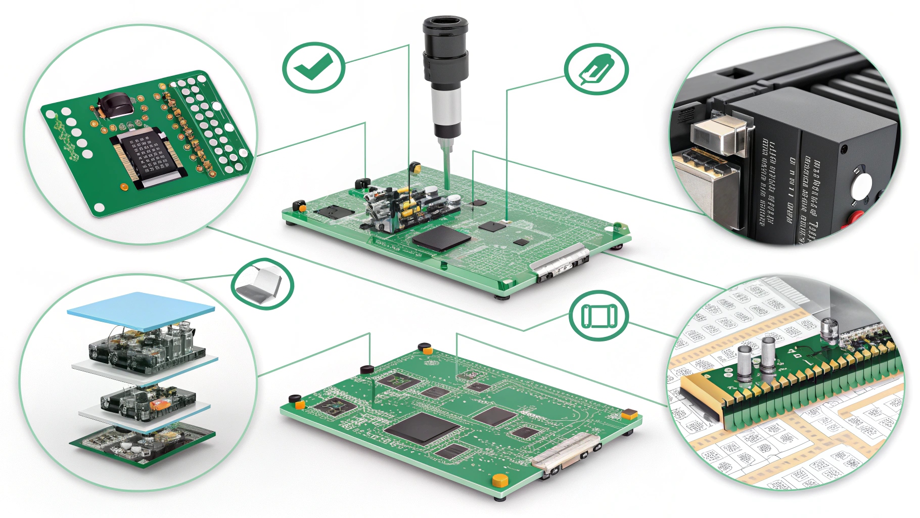
Putting on solder paste is the first and most important step, especially for current electronics that use Surface Mount Technology (SMT) a lot. Think of solder paste as metal glue that sticks to things. This exact mix of small solder particles and flux is what makes electrical links strong. This paste needs to be put on the solder pads, which are exact spots on the PCB where the parts will go.
Most of the time, stenciling is used for this. A thin stainless steel pattern with laser-cut holes that match the PCB’s pad layout is placed directly on top of the board. Solder paste is then spread over the pattern with a squeegee. It’s very important to be exact here.
- If you use too little paste, the link might not be strong enough.
- If you use too much, solder bridges can form and short out nearby parts. This very careful start makes sure that everything that comes next will be strong.
Pick Out and Place 🤖
After the solder paste is carefully put on, it’s time to put the computer parts on the board. With a method called “pick and place,” the power of automation really shines through here. The stars of this show are pick-and-place robots that work quickly. These engineering marvels are fed by reels or trays of parts.
The machine’s head moves back and forth, picking up individual parts from their feeders and placing them exactly where they belong on the solder paste-covered PCB. It does this with the help of several vacuum nozzles or grippers. These machines are guided by advanced vision systems that make sure every part—some of which are smaller than a grain of sand—is in the right place and angled correctly down to the micron level. These days, machines can put together tens of thousands of parts an hour, which makes this step shockingly fast.
Use Reflow Welding to Make it Last Forever 🔥
Once all the surface-mount parts are in their solder paste beds, these connections will be made permanent. One way to do this is with reflow soldering. After being filled with parts, the PCBs are put through a reflow oven, which is a long industrial oven. Different parts of this oven have carefully controlled temperature profiles.
At first, the boards are gradually heated up. This makes it easier for the solder paste to mix with the flux, which cleans the areas that will be soldered and keeps the board and parts from getting too hot. The boards go into the peak reflow zone after being heated up. This is where the temperature rises above the point where solder melts. The small solder particles in the paste melt, or “reflow,” and form strong, irreversible metal bonds between the component leads and the PCB pads. To finish the electrical connections, the boards go through areas that cool down, and the liquid solder sets. This perfectly timed heating and cooling cycle is what keeps every solder joint strong and reliable.
Check and Manage Quality 🧐
After the parts have been bonded together, they need to be carefully inspected to find any problems. Problems can happen even with automated methods that are very accurate.
- Not enough solder can cause open circuits.
- Misaligned components.
- Solder bridges (where a component stands on one end like a small gravestone).
- Tombstoning (where one component stands on top of another).
There are a number of different ways:
- A visual inspection by trained technicians.
- Automated Optical Inspection (AOI) tools are used to check more things and do a better job of it..
- For even more complicated boards, like those with Ball Grid Arrays (BGAs) components, where solder joints are hidden under the component, automated X-ray inspection (AXI) is used.
Through-Hole Assembly💪
Surface Mount Technology is the standard in modern electronics because it makes things smaller, but the old way of putting things together with through hole assembly service is still useful for bigger parts that are subject to mechanical stress, like transformers, plugs, and big capacitors. As part of this process, wires or leads are run through PCB holes that have been drilled in the right order.
After being put in, these leads are attached to the pads on the other side of the board. Technicians who know what they’re doing can do this by hand for small runs or unique parts. Wave soldering is usually used for making things on a bigger scale. Wave soldering involves running the bottom of a PCB over a wave of hot solder while component leads stick out. The solder links the visible leads and pads together in a strong and reliable way. Even though SMT is known for being dense, there are times when through-hole components, which are very strong mechanically, are a must.
Last Checks and Functional Testing ✅
It’s not enough for the assembled PCB to look good; it has to work as planned. This is where functional testing comes in. Custom test tools and software power the board and make it run like it would in the real world. These tests make sure that the PCB does everything it’s supposed to do by checking voltages, data integrity, and general performance. If any board fails these tests, it is sent back to be fixed or reworked so that the problem can be found and fixed.
With this step-by-step guide, you should be able to understand how the PCBA method works. Knowing about these steps helps you understand how hard and carefully gadgets are made. It is very important to look into choices from reputable manufacturers if you want to make your own electronic designs come to life and need professional assembly services. For example, for your next job, a partner like OurPCB might be able to give you the quality and support you need for your next project.